

This article first appeared in the January 1984 issue of VLSI Design magazine. In an industry used to simulating integrated circuits using either a digital logic simulator or an analog simulator like Spice, a hybrid approach like the one I outlined was quite new. These behavioral models became commonplace later on.
With the increase in circuit complexities and the need for very short design times, it is becoming more and more important for a custom or semicustom circuit to work the first time. The sophistication of today’s design-verification tools helps considerably, but only when the design engineers understand the tools and use them properly. Even though modeling might sound simple, many pitfalls await an incorrectly built model. Simulation results must be absolutely trustworthy before expensive manufacturing prototypes can be based on them.
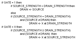
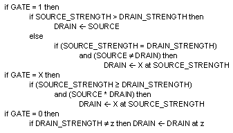
The problems and examples in this article use a standard nine-state logic simulator, as implemented in most of the engineering workstations now on the market (Werner et al. 1983). These nine states actually represent three different logic values at three different strengths, as shown in Table 1. The examples do not use any specific modeling language, but instead are algorithmic descriptions. The sidebar on page 42 shows an example of the same logic function described by behavioral models on several different workstations.

Description of the Algorithmic Language
The language used in these examples is based on Pascal, because most current workstations use a Pascal-like language for behavioral modeling. It has been simplified somewhat for these examples, because the actual programs that read the values from the input pins and place the values on the output pins require much more code than space allowed us to print. The symbols used are shown in Table 2.

Behavioral modeling fits into the design process in several different ways, which often involve different people in the design group. The first use of modeling is for the macros in a standard-cell library or gate-array library. In this case, the model will probably be written by a programmer or technician. The use of a behavioral model here can produce significantly faster and more accurate simulations. “More accurate” in this context means more than just making the appropriate wire take on the right value at the right time; it also means better checking of potential errors, such as clock-phase problems, spikes, set-up and hold time, and refresh-checking on dynamic circuits.
Modeling is also used in the top-down creation of a design. In this case, the design engineers themselves are responsible for specifying (or even writing) the model. This environment is a favorite for demonstrations by the workstation companies that sell modeling tools. The idea is that the systems engineer can draw a block diagram of a large system, with models for each of the blocks. The system is then simulated to ensure that the block diagram is correct before the detailed logic design begins. The blocks are then built, one by one, and tested against their models. This procedure not only ensures that the interfaces between blocks are clean (thus letting several different engineers work on the same circuit), but also lets the blocks be debugged in situ, using models for all of the blocks except the one being tested. The only problem with this approach is that either the systems engineers must know how to program, or else a programmer must be hired to implement the engineers’ concepts.
Third, behavioral modeling is required when the block of circuitry being created cannot be defined in terms of the primitives supplied with the system. One good example is a function such as a Schmitt Trigger, that is “borderline analog.” Whenever behavioral modeling is used in this context, the circuit should be analyzed very carefully using a circuit simulator (such as SPICE or ASPEC) to ensure that the behavioral model accurately represents what the circuit itself is supposed to do.
Modeling Standard Parts
Perhaps the most basic one of all the functions required in an MOS circuit, yet one of the most difficult to model, is the transistor (Figure 1). For almost all applications, we can view it as being unidirectional, with the input being its source, and the output being its drain. In a drastically simplified view of a FET, when the gate is ON (logical 1 on an n-channel MOSFET), the source and drain are connected; and when the gate is OFF, they are not.

This simplistic view of the transistor has several problems. The first is that it does not deal with an unknown gate. Second, in a standard nine-state simulator, there is no such thing as an open circuit. The drain will always produce some kind of output, even when the gate is zero. The third problem is that because dynamic logic relies heavily on nodal capacitance, the state of the drain depends on more than just the state of the other two pins. We will examine these problems one by one.
An “unknown” gate means simply that we do not know whether the transistor is ON or OFF. If the source is at a different potential than the drain, a problem might occur. The solution could be expressed in the following way:
In other words, whenever the gate is ON and the signal at the source node of the transistor is stronger than the signal at the drain, the source will be able to overpower the drain If the strengths are the same (and the signals are not), the result will be a “fight” between the source node and the drain node, with one trying to pull up and the other trying to pull down. In this case, the drain is set to an unknown value at the same strength it previously had. If the signal on the drain is stronger than the signal on the source, the drain value will not change; hence, the program does not need a statement to cover this condition. We only care whether the gate is unknown if the source and drain are at different potentials, and if the drain is not overpowering the source.
What this example leaves out is the condition in which the gate is OFF. It would be nice to say, “don’t do anything here,” but in reality, the simulator will continue to force onto the drain whatever value it had been putting there, until we tell it differently. But in a real n-channel FET, there is some capacitance on the drain. This means that when the gate is turned off, the value that was on that net remains for a while, even though there isn’t much drive behind it. We can simulate this condition by adding a clause to our model that sets the drain to its same value, but at a high-impedance strength:

Although it would be nice to think that the addition of some capacitance means that the model will work for dynamic logic (as mentioned above), some work remains to be done. For example, consider how the dynamic shift register shown in Figure 2 will behave using this model. (Assume that the model for the pMOS device is the same as that for the nMOS device, except that a “0” turns the gate ON and a “1” turns it OFF.)

The shift register works in the following way. When the clock is HIGH (and its complement is LOW), then transistors P3 and N3 will be ON, letting transistors P4 and N4 act as an inverter, placing at the output the complement of the value stored at the node called “STORAGE.” Because P1 and Nl will be OFF, the storage node is driven only by its inherent capacitance. When the clocks change state, P1 and N1 are turned ON (letting P2 and N2 act as an inverter transferring the inverse of the input signal to the storage node), and P3 and N3 are turned OFF (disconnecting the storage node from the output).
If we try to simulate this structure with our current transistor model, we run into a major problem. The source node of N1 can never have any value other than 0, and the source node of P1 will always have a value of 1. Therefore, whenever P1 and N1 are turned OFF, the drains of P2 and N2 go to opposite values at a high-impedance strength. The resulting conflict produces Xz on the storage node, regardless of the value that should be stored there.
To solve this problem, we must model the capacitor on the drain of any MOS device more intelligently. When the gate of the device is OFF, any other signal that changes state and is connected to the drain (and is stronger than “high impedance”) should predominate. Our resulting model looks like this:
But even this model does not provide an ideal definition of the workings of an n-channel FET. The remaining considerations that this model does not take into account include the fact than in order to be turned ON, an n-channel device requires more than just a 1 on the gate. Current must also flow between the drain and the source. Furthermore, for proper modeling of a transmission switch created from a pMOS device and an nMOS device, the models should be bidirectional.
Our goal is not to replace SPICE with a logic simulator, but instead to let digital design engineers build and analyze logic functions made up of transistors. The engineers must still use a circuit simulator to find out how fast such logic functions will operate.
Modeling Blocks in a Hierarchy
The modeling of blocks can involve elements as simple as the equality block described in the sidebar on page 42, all the way up to entire subsystems. Theoretically, it is possible to model any digital function using modeling languages that exist today, with the only limit being that of performance. Extrapolations of smaller simulations indicate that if one were to go so far as to model the processor that runs the simulator (in this case, the Motorola MC 68000), approximately 106 real processor cycles would be needed to model each simulated processor cycle.
Some functions lend themselves well to behavioral modeling, and some do not. The classic example of a function that is easier to describe with logic than with a model is a block of random logic liberally sprinkled with flip-flops and latches. Functions that are easy to describe are those that perform a single operation, however complex. For example, the design of an 8-bit synchronous up-down counter with asynchronous reset can become quite a complex job. Having a design drawn up for a 6-bit version of this counter might help, but a good bit of logic-design work would remain to be done. On the other hand, a well-written model would require only the changing of a single constant.
The simplicity of the model depends on how well thought-out the problem is before programming begins. If the function is very well understood, one needs only to describe it in short, simple, English-language statements. This way, a program statement in the model will correspond to each English-language statement. The model for the counter described above is shown below:

Q is the output, and DIRECTION and RESET are inputs. Code still would have to be written to detect the active clock edge. This model assumes that the behavioral language being used can understand buses as a single entity rather than as a set of discrete lines. If the modeling language does not have this capability, then it is much simpler to have a translator convert the individual bits into an integer, and convert the integer back to bits when you output it.
In such a case, another advantage of a model is that it is very easy to change the model as you add other capabilities to the system design. Only after the entire system is functional need you be concerned with designing the logic. For example, the program excerpt that appears below shows this same model, changed so that it can be SET asynchronously and parallel loaded synchronously:

Note that we must be careful to check not only for one and zero, but also for the unknown condition; and that if both SET and RESET are ON at once, or if either of them has an unknown value, then we set the output to UNKNOWN. We only check for an unknown LOAD when SET and RESET are both inactive, and when there is an active clock edge, because these are the conditions under which this parameter makes any difference. DIRECTION matters only if all of the foregoing conditions hold true and if LOAD is inactive.
However, the engineer must remember that in order for the simulation to be meaningful, the model must include realistic delay times. If the model can run at 200 MHz, but the silicon is good only up to 20 MHz, you would be better off without the model.
Modeling Non-Digital Functions
In trying to model non-digital functions using a logic simulator. we are once again treading on the traditional territory of the circuit simulator. Many simple pseudo-analog functions are often used in circuits that are otherwise completely digital, and it is convenient to be able to simulate an entire circuit as a whole. Even on a mainframe computer, it is not cost-effective (nor even always possible) to simulate an entire circuit using SPICE or ASPEC, especially when you are working with some of the large circuits being built today. A typical 1000-gate CMOS gate-array chip can contain more than 4,500 transistors, and many circuits are considerably larger than that.
Again, our intention is not to replace the circuit simulator, but instead to use the circuit simulator to characterize functions so that they can later be modeled with the logic simulator. As an example, we will examine a Schmitt Trigger. A Schmitt Trigger is merely a buffer (or inverter) that has widely separated high-going and low-going thresholds. The net effect is that a non-inverting Schmitt Trigger will go HIGH only when the input rises above 2.4 volts, and will go LOW only when the input falls below 0.7 volts. In this example, all of the thresholds must be worked out carefully before we can prepare a behavioral model of the Schmitt Trigger.
This function is traditionally modeled in a logic simulator as an ordinary delay gate that does nothing to the line except cause a slight delay. If given ordinary digital inputs, that is exactly what the Schmitt Trigger will do. But in the case that we want to simulate, the transitions are not clean. The purpose of a Schmitt Trigger is to make sure that the output undergoes only one transition when the input is either drifting up and down, or drifting away from the power supply (when it should stay there).
The analog signal can be modeled in several different ways, all of which require a bus instead of a single wire. Perhaps the simplest way to model this function is to have the bus represent the voltage on the input in binary notation and in units of one tenth of a volt. For a typical 5-volt system, this technique would require a 6-bit bus. (Six binary digits can represent the numbers from 0 to 63, thus indicating values from 0 volts to 6.3 volts.) The model would read as shown below:

However, not all modeling languages are able to treat a bus as a binary number. In many cases, the bus value will have to be converted by a short routine on the input, and converted back by a corresponding routine on the output. Such an input-conversion routine would read as shown below:

This representation of an analog signal using a binary number on a bus allows high resolution without much cost (hundredth-volt resolution would require only 9 bits on the bus, for a range of 0 to 5.11 volts), and would make it very easy to model functions such as digital-to-analog conversion.
Mentor’s logic simulator has a different way of displaying a bus, which leads us to a different way to represent the bus internally. In the Mentor system, a bus is shown as a series of superimposed waveforms of differing amplitudes, so that the “1” value for the lowest-order bit (bit 0) is at the bottom, and the “1” for the highest-order bit is at the top. The analog signal can be represented by setting a single bit on the bus to represent each value. In the first example given above, the bus would be a 51-bit bus, in which each bit represents a 0.1 volt increment. If the value on the input were 0 volts, bit 0 (only) of the bus would be a 1. If the value on the input were 5 volts, bit 50 would be a 1. This method produces a visually pleasing analog waveform (see Figure 3).

assignment of an analog signal to a 51-bit bus.
This method uses considerably more space (51 bits instead of 6), but one of its assumptions is that the circuit being simulated is primarily digital, with only a few analog components. The additional storage required by larger buses is one byte per bit. Therefore, a circuit with ten 51-bit buses would require 450 bytes more than a circuit with ten 6-bit buses. This amount is a small percentage of the standard 1.5 megabytes of real memory, and an even smaller percentage of a 16-megabyte virtual memory.
Conclusion
We are only beginning to explore the immense potential of behavioral modeling. As users become more sophisticated, and as engineers become more software-savvy, modeling will become an integral part of day-to-day design, and design throughput will improve.
Whenever behavioral models are not standard parts of a library, or have not been fully characterized, care must be taken to simulate the entire circuit without models. There is a great potential for error in programming models to do things that cannot be done in silicon. In a large system, after all of the individual blocks have been simulated successfully, and after their models have been simulated together, it is tempting to assume that the blocks will work together. But subtle differences in timing can be deadly.
Sidebar

References
Werner, J., G. Robson, and R. Harris. November 1983. “Comparing the Computer-Aided Engineering Systems in Action,” VLSI DESIGN.
